
 English
IP in Semiconductor technology – Overview
Semiconductor technology is deeply embedded in today’s digital economy. It has played a major role in spurring innovation, productivity and economic growth. Intellectual Property (IP) has been the lifeblood of semiconductor industry in the past four decades. In the first of a series of upcoming articles, we will take a deep dive into the role played by IP in shaping the semiconductor innovation ecosystem beginning from early-stage invention and first commercialization to mass production and diffusion. Although early stage innovation relies heavily on contributions in fundamental science, linkages to public research and individual entrepreneurship, IP in the form of patents have been an effective tool for sharing innovative technology and increasing productivity by efficiently using R&D resources.
As semiconductor technology evolved from transistor era to present day neural core processors in multiple phases, the evolution coincided with rise in patent filings. Patents also facilitated specialization and helped to mobilize resources to cover the high R&D costs and to finance startups. The key reason of high R&D cost has been high setup cost of fabrication facility and sourcing of raw materials. It is also the reason behind current slowdown in Moore’s law and competitive advantage of 7 nm over 10 nm devices. In this present article, we will try to get a broader view of patent landscape in fabrication technology.
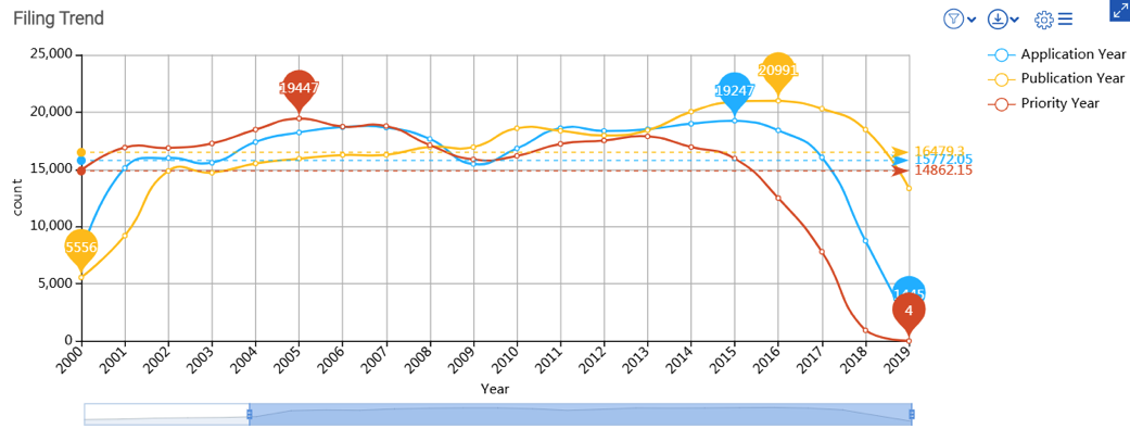
Figure 1 Filing Trend in Semiconductor Fabrication in last 2 decades
As we can infer from Figure 1, the filing trend in fabrication has come down since 2015, which points to a slowdown of Moore’s law and the diminishing returns on further investing in high cost fabrication facility. It also highlights the technological challenges related to quantum tunneling that starts to play a major role as we reduce the channel length below 10 nm.

Figure 2 Key areas of Patent filing in Semiconductor technology in last 2 decades
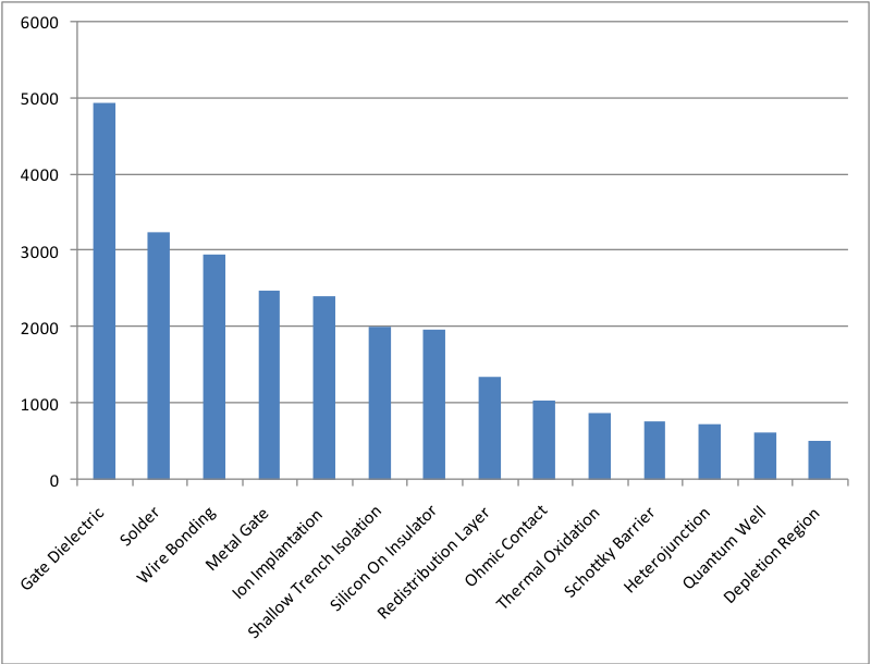
Figure 3 Key areas of Patent filing in Semiconductor technology since 2015
If we compare the filing trends in the last two decades (Fig 2) with the filing trend since 2015 (Fig 3), the technologies which are playing a major role below 10 nm can be easily determined. Among these Gate dielectric is one of the prominent as it determines the amount of leakage current flowing across the transistor terminals. Packaging technology is another one which has got a lot of attention from the inventors due to its relevance in 5G.
As we continue to track the patent filing activity across different domains by different players on Dolcera’s AI enabled analytics tool Patent Categorization System (PCS), we develop a broader picture of technology trends in semiconductor fabrication landscape. Based on this information, it is easier to conclude that both technological constraints and diminishing Return on Investment in specific fabrication domains can shape the future of our digital economy. In the upcoming articles, we will make a deeper dive into each of those key technologies and try to get a better understanding on the effect of these constraints on different markets. Based on this understanding, IP strategies can be developed to capitalize on market dynamics with higher accuracy.
PCS is Dolcera’s flagship patent analytics platform. With a corpus of over 110 million worldwide patents updated daily, PCS provides answers to every patent question in detail and blindingly fast.

For more queries, feel free to visit us at http://dolcera.com/
