Difference between pages "Carbon Nanotubes (CNT)" and "Pressure sensitive adhesives"
(→Applications of Nanotechnology) |
(→Taxonomy for analysis) |
||
| Line 1: | Line 1: | ||
| − | == | + | ==Dashboard== |
| + | Dolcera dahsboard provides quick and easy navigation through the technology segments. Below is the snapshot of how it look like. Click on the link [http://client.dolcera.com/dashboard/dashboard.html?workfile_id=262 '''Dolcera Dashboard'''] for Pressure Sensitive Adhesives. | ||
| + | [http://client.dolcera.com/dashboard/dashboard.html?workfile_id=262 '''Dolcera Dashboard'''] | ||
| − | + | [[image:dashboard.jpg|center|500 px]] | |
| − | + | ||
| − | == | + | ==Overview== |
| − | + | Pressure sensitive adhesive (PSA, self adhesive, self stick adhesive) is adhesive that forms a bond when pressure is applied to marry the adhesive with the adherend. No solvent, water, or heat is needed to activate the adhesive. It is used in pressure sensitive tapes, labels, note pads, automobile trim, and a wide variety of other products. | |
| − | + | ||
| − | + | ||
| − | + | ||
| − | + | ||
| − | + | ||
| − | + | As the name "pressure sensitive" indicates, the degree of bond is influenced by the amount of pressure which is used to apply the adhesive to the surface. | |
| − | + | ||
| − | + | Surface factors such as smoothness, surface energy, removal of contaminants, etc. are also important to proper bonding. | |
| − | + | ||
| − | + | ||
| − | + | ||
| − | + | ||
| − | + | ||
| − | + | ||
| − | + | ||
| − | + | ||
| − | + | ||
| − | + | ||
| − | + | ||
| − | + | ||
| − | + | ||
| − | + | ||
| − | + | ||
| − | + | PSAs are usually designed to form a bond and hold properly at room temperatures. PSAs typically reduce or lose their tack at cold temperatures and reduce their shear holding ability at high temperatures: Specialty adhesives are made to function at high or low temperatures. It is important to choose an adhesive formulation which is designed for its intended use conditions. | |
| − | [http://www. | + | ===Surface Energy=== |
| + | [[Image:Surface energy.jpg|thumb|right|800|Measuring of Surface Energy]] | ||
| + | # Surface energy is a measure of how well an adhesive wets out over the surface of the material to which it is applied. | ||
| + | # The most common method of determining the surface energy is to measure the contact angle of a water droplet on the substrate surface. | ||
| + | # The contact angle between the solid and the fluid is the angle measured within the fluid, between the solid surface and the tangent plane to the liquid surface at the point of intersection. | ||
| + | # A contact angle of greater than 90° indicates that the fluid (which is ink or adhesive in this case) has not wet the surface. Conversely an angle of less than 90° means that the fluid has wet the surface - if the angle approaches zero then the surface is completely wetted by the fluid. | ||
| + | # The surface energy or the wetability of a particular substrate is measured in dynes/cm. [http://images.google.com/imgres?imgurl=http://www.pcn.org/images/Technical%2520Notes%2520-%2520Corona1.jpg&imgrefurl=http://www.pcn.org/Technical%2520Notes%2520-%2520Corona.html&h=327&w=370&sz=13&hl=en&start=2&um=1&tbnid=Nb4kgRrPYnxojM:&tbnh=108&tbnw=122&prev=/images%3Fq%3Dsurface%2Benergy%26svnum%3D10%26um%3D1%26hl%3Den%26sa%3DX Source] | ||
| + | ===Low Surface Energy Substrates=== | ||
| + | # Low energy plastics, such as polypropylene (PP), polyethylene (PE) and Teflon (PTFE) are essentially "non- stick" plastics. | ||
| + | # Their molecular structure inhibits the adhesion and printing processes - this molecular structure is basically inert or inactive – these polymers are said to have a low surface energy. | ||
| + | # Materials with low surface energy (LSE) do not allow adhesives to wet out, while materials with high surface energy (HSE) provide excellent wet-out, providing the best adhesion. | ||
| + | # Rubber-based adhesives usually provide better adhesion to LSE surfaces. | ||
| + | # Some substrates require special treatment such as corona treating, primers, top coating, etc., in order to achieve better adhesion. | ||
| + | # On some LSE substrates, adhesion levels improve the longer adhesive is applied. [http://www.chemsultants.com/latestprods/adhesive_definitions.html Source] | ||
| − | + | ===Adhesion=== | |
| − | + | [[Image:Adhesionnew.jpg|thumb|right|800|Adhesion]] | |
| − | + | # Adhesion is the molecular force of attraction between unlike materials. | |
| − | + | # Adhesion and cohesion, attractive forces between material bodies. A distinction is usually made between an adhesive force, which acts to hold two separate bodies together (or to stick one body to another) and a cohesive force, which acts to hold together the like or unlike atoms, ions, or molecules of a single body. | |
| − | + | # For example water molecules stick to each other. This is caused by hydrogen bonds that form between the slightly positive and negative ends of neighboring molecules. | |
| − | + | # Water is found in drops; perfect spheres. It’s hard to imagine water behaving any other way due to cohesion and water molecules stick to other surfaces due to adhesion.[http://images.google.com/imgres?imgurl=http://www.ccs.k12.in.us/chsBS/kons/kons/images/water-droplet.jpg&imgrefurl=http://www.ccs.k12.in.us/chsBS/kons/kons/physical_properties_of_water.htm&h=168&w=238&sz=15&hl=en&start=4&tbnid=UrmkX2TGv_os2M:&tbnh=77&tbnw=109&prev=/images%3Fq%3Dwater%2Badhesion%26gbv%3D2%26svnum%3D10%26hl%3Den%26sa%3DG Source] | |
| − | + | ||
| − | + | ||
| − | + | ||
| − | + | ||
| − | + | ||
| − | + | ||
| − | + | ||
| − | + | ||
| − | + | ||
| − | + | ||
| − | + | ||
| − | + | ||
| − | + | ||
| − | + | ||
| − | + | ||
| − | + | ||
| − | + | ||
| − | + | ||
| − | + | ||
| − | + | ||
| − | + | ||
| − | + | ||
| − | + | ||
| − | + | ||
| − | + | ||
| − | + | ||
| − | + | ||
| − | + | ||
| − | + | ||
| − | + | ||
| − | + | ||
| − | + | ||
| − | + | ||
| − | + | ||
| − | + | ||
| − | + | ||
| − | + | ||
| − | [ | + | ===Pressure Sensitive Adhesive(PSA)=== |
| + | # Pressure sensitive adhesives are adhesives that adhere to a variety of substrates when applied with pressure. | ||
| + | # The primary mode of bonding for a pressure sensitive adhesive is not chemical or mechanical but polar attraction to the substrate surface. | ||
| + | # Applied pressure is necessary in order to achieve sufficient wet-out onto the substrate surface to provide adequate adhesion. [http://www.chemsultants.com/latestprods/adhesive_definitions.html Source] | ||
| − | |||
| − | + | [[image: Sealeant in adhesive.jpg|center|500 px]] | |
| − | [[ | + | |
| − | + | ==Market Information== | |
| − | + | * According to a report from the Business Communications Company, the 2001 US market for specialty adhesives was about $5.7 billion, and is forecast to grow at 4.3% per year, with medical and dental applications being the fastest-growing sector at 5.9% per year. [http://www.marketfile.com/print/paint/title5/index.htm Source] | |
| + | * Frost and Sullivan report the size of the European PSA market (medical and non-medical) to be $620 million in 2000, forecast to grow to $796 million in 2007. [http://www.engineeringtalk.com/news/fro/fro122.html Source] | ||
| + | * The world value of the overall adhesives market is estimated at US $22 billion. | ||
| + | * '''Total Market Expected to Grow at a CAGR of 9 Percent''': The U.S. PSA markets for labels and narrow-web graphics is expected to growth with a CAGR of 9 percent during the years 2006–2012. The total U.S. PSA markets for labels and narrow-web graphics unit shipments are expected to continue to growth at a CAGR of 6.6 percent due to high end-user growth. The UV technology is a new technology that have started to receive wide acceptance in the industry and that segment of the industry is a fragmented and developing segment with growth rates in double digits. While the solvent-based PSAs are expected to show decreasing growth percents, the water-based and solvent-based segments are expected to growth in the lines of the total industry. [http://www.frost.com/prod/servlet/report-brochure.pag?id=F652-01-00-00-00 Source] | ||
| − | + | * According to '''World Adhesives File 2000-2005''', the leading handful of adhesives suppliers, including pressure sensitive companies, already controlled almost half the global market in 1999. Henkel leads the way with an estimated 12% global market share, which will probably increase to around 14% with the purchase of Dexter’s adhesives interests. Pressure sensitive suppliers 3M and Avery Dennison are ranked second and third, with 9% and 7% shares respectively, followed jointly by National Starch and H.B. Fuller — both at 6%. The newly enlarged Atofina and Rohm and Haas follow closely behind.” [http://answers.google.com/answers/threadview?id=60487 Source] | |
| − | + | * Growth of the world market averages about 2-3% per year. | |
| − | + | * Packaging adhesives make up the majority of the market. | |
| − | + | * The electronic and medical adhesives market is currently experiencing the most rapid growth. | |
| − | and | + | |
| − | + | * Market leaders by country are as follows: | |
| − | + | ** United States - approximately 2.6 tonnes annually | |
| − | [[ | + | ** China |
| − | + | ** Japan | |
| − | + | ** Germany | |
| − | + | ** UK [[image:players_logo.jpg|right|500 px]] | |
| − | + | * Market leaders by company(which account for one-third of the market share) are: | |
| − | + | ** Henkel | |
| − | + | ** 3M | |
| − | + | ** Avery Denison | |
| − | + | ** HB Fuller | |
| − | + | ** National Starch | |
| − | + | ** Atofina | |
| − | + | ||
| − | + | ||
| − | + | ||
| − | + | ||
| − | + | ||
| − | + | ||
| − | + | ||
| − | + | ||
| − | + | ||
| − | + | ||
| − | + | ||
| − | + | ||
| − | + | ||
| − | + | ||
| − | + | ||
| − | + | ||
| − | + | ||
| − | + | ||
| − | + | ||
| − | + | ||
| − | + | ||
| − | + | ||
| − | + | ||
| − | + | ||
| − | + | ||
| − | + | ||
| − | + | ||
| − | + | ||
| − | + | ||
| − | + | ||
| − | + | ||
| − | + | ||
| − | + | ||
| − | + | ||
| − | + | ||
| − | === | + | ==Intellectual Property== |
| − | + | ||
| − | + | ||
| − | + | ||
| − | == | + | ===Patent Search Table=== |
| − | + | {|border="1" cellspacing="0" cellpadding="4" width="100%" | |
| − | + | |colspan = "5"| | |
| − | + | * Patent search on Micropat | |
| − | + | * Databases searched: '''USG USA EPA EPB WO JP DEG DEA DET DEU GBA FRA''' | |
| − | + | ||
| − | + | ||
| − | + | ||
| − | + | ||
| − | + | ||
| − | + | ||
| − | + | ||
| − | == | + | |
| − | + | ||
| − | + | ||
| − | + | ||
| − | + | ||
| − | + | ||
| − | + | ||
| − | + | ||
| − | + | ||
| − | + | ||
| − | + | ||
| − | + | ||
| − | + | ||
| − | + | ||
| − | + | ||
| − | + | ||
| − | + | ||
| − | + | ||
| − | + | ||
| − | + | ||
| − | + | ||
| − | {|border=" | + | |
| − | | | + | |
| − | + | ||
| − | + | ||
| − | + | ||
| − | + | ||
| − | + | ||
| − | + | ||
| − | + | ||
| − | + | ||
| − | + | ||
| − | + | ||
| − | + | ||
| − | + | ||
| − | + | ||
| − | + | ||
| − | + | ||
| − | + | ||
| − | + | ||
| − | + | ||
|- | |- | ||
| − | | | + | |bgcolor = "#FFFF99"|'''Query.No.''' |
| − | | | + | |bgcolor = "#FFFF99"|'''Searched Sections''' |
| − | | | + | |bgcolor = "#FFFF99"|'''Years Searched''' |
| + | |bgcolor = "#FFFF99"|'''Query''' | ||
| + | |bgcolor = "#FFFF99"|'''Hits''' | ||
|- | |- | ||
| − | | | + | |1 |
| − | | | + | |Claims, Title or Abstract |
| − | | | + | |1836 – Date |
| + | ||(rubber OR acryl* OR silicone OR oil*1 OR resin*1 OR ethylen* OR isoprene OR terpene OR copolymer* OR vinyl* OR siloxane* ((acid OR anhydride) ADJ1 (acrylic OR crotonic OR (vinyl ADJ1 acetic) OR fumaric OR maleic OR malonic OR succinic OR itaconic OR citraconic)) OR polymer* OR styrene OR ester*) SAME (((pressure ADJ1 sensitive) NEAR2 (adhesive* OR glue OR paste OR (binding ADJ1 agent) OR (epoxy ADJ1 resin*) OR film) OR PSA OR PSAs) OR (adhesion* WITH (peel OR tensile OR shear) OR stick*) OR (radical* ADJ1 (initiator* OR maker*))) | ||
| + | |76006 | ||
|- | |- | ||
| − | | | + | |2 |
| − | | | + | |Claims, Title or Abstract |
| − | | | + | |1836 – Date |
| + | |(((low ADJ surface ADJ energy) WITH (substrate*1 OR polymer OR compound* OR material OR film)) OR (surface ADJ1 tension) OR (surface ADJ1 rough*) OR viscosity OR (oily ADJ surface) OR (low ADJ1 energy ADJ1 surface*)) AND (polyolefin*1 OR polyethylene*1 OR polypropylene*1 OR (polyvinyl ADJ1 chloride ADJ1 film) OR (oil ADJ1 contaminated ADJ1 metal) OR polybutene OR polyisoprene*1 OR (polyvinylidene ADJ1 fluoride*) OR polytetrafluoroethylene*1 OR polyester*1 OR polyamide*1 OR polyacetal*1 OR polystyrene*1 OR polyurethane* OR polyurea OR silan* OR polycarbonate*) | ||
| + | |75602 | ||
|- | |- | ||
| − | | | + | |3 |
| − | | | + | |Claims, Title or Abstract |
| − | + | |1836 – Date | |
| − | + | |1 AND 2 | |
| − | + | |2272 | |
| − | + | ||
| − | + | ||
| − | | | + | |
| − | | | + | |
| − | | | + | |
| − | + | ||
|- | |- | ||
|} | |} | ||
| + | * Total number of patents - 2272 | ||
| + | * Total number of unique patent families - 1483 | ||
| + | ===Taxonomy for analysis=== | ||
| + | [[Image:adhesion-3Mnew2.jpg|thumb|center|800px|Taxonomy map - Adhesion]] | ||
| − | + | ===Taxonomy for PSA composition=== | |
| − | + | [[Image:adhesion-final version.jpg|thumb|center|1000px|Taxonomy map - Adhesion]] | |
| − | + | ||
| − | + | ||
| − | + | ||
| − | + | ||
| − | == | + | |
| − | + | ||
| − | + | ||
| − | + | ||
| − | + | ||
| − | = | + | |
| − | + | ||
| − | + | ||
| − | [[Image: | + | |
| − | + | ||
| − | + | ||
| − | + | ||
| − | + | ||
| − | + | ||
| − | + | ||
| − | + | ||
| − | + | ||
| − | + | ||
| − | + | ||
| − | + | ||
| − | + | ||
| − | + | ||
| − | + | ||
| − | + | ||
| − | === IP Activity | + | ===IP Activity=== |
| + | [[image:Priority year_PSA.jpg|center|600 px|thunb|Competitors]] | ||
| + | ===Major Competitors=== | ||
| + | [[image:competitors_PSA.jpg|center|600 px|thunb|Competitors]] | ||
| − | + | ===Composition components matrix=== | |
| − | + | ||
| − | + | ||
| − | + | ||
| − | === | + | |
| − | + | ||
{|border="2" cellspacing="0" cellpadding="4" width="100%" | {|border="2" cellspacing="0" cellpadding="4" width="100%" | ||
| − | |align = " | + | |align = "center" bgcolor = "#C0C0C0"|'''Assignees''' |
| − | |align = " | + | |align = "center" bgcolor = "#C0C0C0"|'''Rubber''' |
| − | |align = " | + | |align = "center" bgcolor = "#C0C0C0"|'''Silicone''' |
| − | |align = " | + | |align = "center" bgcolor = "#C0C0C0"|'''Polymers''' |
| − | |align = " | + | |align = "center" bgcolor = "#C0C0C0"|'''Acrylic''' |
| − | |align = " | + | |align = "center" bgcolor = "#C0C0C0"|'''Tackifying resin''' |
| − | |align = " | + | |align = "center" bgcolor = "#C0C0C0"|'''Plasticizer oil''' |
| + | |align = "center" bgcolor = "#C0C0C0"|'''Carboxylic acids''' | ||
| + | |align = "center" bgcolor = "#C0C0C0"|'''Acid Esters''' | ||
| + | |align = "center" bgcolor = "#C0C0C0"|'''Priority Year''' | ||
| + | |align = "center" bgcolor = "#C0C0C0"|'''Patent numbers''' | ||
|- | |- | ||
| − | | | + | |rowspan = "3"|3M Innovative Properties Company |
| − | |align = " | + | |align = "center"|x |
| − | |align = " | + | |align = "center"| |
| − | |align = " | + | |align = "center"|x |
| − | |align = " | + | |align = "center"|x |
| − | |align = " | + | |align = "center"|x |
| − | |align = " | + | |align = "center"|x |
| + | |align = "center"| | ||
| + | |align = "center"| | ||
| + | |2000 | ||
| + | |<font color="#0000FF"><u>[http://patft.uspto.gov/netacgi/nph-Parser?patentnumber=6630531 US6630531]</u></font> | ||
|- | |- | ||
| − | |align = " | + | |align = "center"|x |
| − | |align = " | + | |align = "center"| |
| − | |align = " | + | |align = "center"|x |
| − | |align = " | + | |align = "center"|x |
| − | |align = " | + | |align = "center"|x |
| − | |align = " | + | |align = "center"| |
| − | |align = " | + | |align = "center"| |
| + | |align = "center"| | ||
| + | |2000 | ||
| + | |<font color="#0000FF"><u>[http://patft.uspto.gov/netacgi/nph-Parser?patentnumber=6632872 US6632872]</u></font> | ||
|- | |- | ||
| − | |align = " | + | |align = "center"| |
| − | |align = " | + | |align = "center"| |
| − | |align = " | + | |align = "center"|x |
| − | |align = " | + | |align = "center"|x |
| − | |align = " | + | |align = "center"| |
| − | |align = " | + | |align = "center"| |
| − | |align = " | + | |align = "center"| |
| + | |align = "center"| | ||
| + | |2000 | ||
| + | |<font color="#0000FF"><u>[http://patft.uspto.gov/netacgi/nph-Parser?patentnumber=6455634 US6455634]</u></font> | ||
|- | |- | ||
| − | |align = " | + | |American Tape Company |
| − | |align = " | + | |align = "center"|x |
| − | |align = " | + | |align = "center"| |
| − | |align = " | + | |align = "center"| |
| − | |align = " | + | |align = "center"| |
| − | |align = " | + | |align = "center"| |
| − | |align = " | + | |align = "center"|x |
| + | |align = "center"| | ||
| + | |align = "center"| | ||
| + | |1997 | ||
| + | |<font color="#0000FF"><u>[http://patft.uspto.gov/netacgi/nph-Parser?patentnumber=5798175 US5798175]</u></font> | ||
|- | |- | ||
| − | |align = " | + | |Ashland Oil, Inc. |
| − | |align = " | + | |align = "center"|x |
| − | |align = " | + | |align = "center"| |
| − | |align = " | + | |align = "center"|x |
| − | |align = " | + | |align = "center"|x |
| − | |align = " | + | |align = "center"| |
| − | |align = " | + | |align = "center"| |
| + | |align = "center"| | ||
| + | |align = "center"| | ||
| + | |1991 | ||
| + | |<font color="#0000FF"><u>[http://patft.uspto.gov/netacgi/nph-Parser?patentnumber=5434213 US5434213]</u></font> | ||
|- | |- | ||
| − | | | + | |rowspan = "4"|Atlantic Richfield Company |
| − | |align = " | + | |align = "center"| |
| − | |align = " | + | |align = "center"| |
| − | |align = " | + | |align = "center"|x |
| − | |align = " | + | |align = "center"|x |
| − | |align = " | + | |align = "center"|x |
| − | |align = " | + | |align = "center"|x |
| + | |align = "center"| | ||
| + | |align = "center"| | ||
| + | |1984 | ||
| + | |<font color="#0000FF"><u>[http://patft.uspto.gov/netacgi/nph-Parser?patentnumber=4656213 US4656213]</u></font> | ||
|- | |- | ||
| − | |align = " | + | |align = "center"|x |
| − | |align = " | + | |align = "center"| |
| − | |align = " | + | |align = "center"|x |
| − | |align = " | + | |align = "center"|x |
| − | |align = " | + | |align = "center"|x |
| − | |align = " | + | |align = "center"| |
| − | |align = " | + | |align = "center"| |
| + | |align = "center"| | ||
| + | |1996 | ||
| + | |<font color="#0000FF"><u>[http://patft.uspto.gov/netacgi/nph-Parser?patentnumber=5817426 US5817426]</u></font> | ||
|- | |- | ||
| − | |align = " | + | | |
| − | |align = " | + | |align = "center"| |
| − | |align = " | + | |align = "center"|x |
| − | |align = " | + | |align = "center"|x |
| − | |align = " | + | |align = "center"|x |
| − | |align = " | + | |align = "center"| |
| − | |align = " | + | |align = "center"| |
| − | | | + | |align = "center"| |
| − | | | + | |1996 |
| − | + | |<font color="#0000FF"><u>[http://patft.uspto.gov/netacgi/nph-Parser?patentnumber=5817426 US5817426]</u></font> | |
| − | + | ||
| − | + | ||
| − | + | ||
| − | + | ||
| − | + | ||
|- | |- | ||
| − | |||
| − | |||
| − | |||
| − | |||
| − | |||
| − | |||
| − | |||
| − | |||
| − | |||
| − | |||
| − | |||
| − | |||
| − | |||
| − | |||
| − | |||
| − | |||
| − | |||
| − | |||
| − | |||
| − | |||
| − | |||
| − | |||
| − | |||
| − | = | + | |align = "center"|x |
| − | + | |align = "center"| | |
| − | + | |align = "center"| | |
| − | + | |align = "center"|x | |
| − | + | |align = "center"| | |
| − | + | |align = "center"| | |
| − | + | |align = "center"| | |
| − | + | |align = "center"| | |
| − | + | |1997 | |
| − | + | |<font color="#0000FF"><u>[http://patft.uspto.gov/netacgi/nph-Parser?patentnumber=6461707 US6461707]</u></font> | |
| − | + | ||
| − | + | ||
| − | + | ||
| − | + | ||
| − | + | ||
| − | |align = "center" | + | |
| − | |align = "center" | + | |
|- | |- | ||
| − | |align = "center"|[http:// | + | |Coloplast |
| − | + | |align = "center"|x | |
| + | |align = "center"| | ||
| + | |align = "center"|x | ||
| + | |align = "center"| | ||
| + | |align = "center"|x | ||
| + | |align = "center"| | ||
| + | |align = "center"| | ||
| + | |align = "center"| | ||
| + | |1980 | ||
| + | |<font color="#0000FF"><u>[http://patft.uspto.gov/netacgi/nph-Parser?patentnumber=6437038 US6437038]</u></font> | ||
|- | |- | ||
| − | |align = "center"| | + | |rowspan = "5"|Dow Corning Corporation |
| − | |align = "center"| | + | |align = "center"| |
| + | |align = "center"|x | ||
| + | |align = "center"|x | ||
| + | |align = "center"| | ||
| + | |align = "center"| | ||
| + | |align = "center"|x | ||
| + | |align = "center"| | ||
| + | |align = "center"| | ||
| + | |1970 | ||
| + | |<font color="#0000FF"><u>[http://patft.uspto.gov/netacgi/nph-Parser?patentnumber=5916981 US5916981]</u></font> | ||
|- | |- | ||
| − | |align = "center"| | + | | |
| − | |align = "center"| | + | |align = "center"|x |
| − | | | + | |align = "center"|x |
| − | |align = "center"| | + | |align = "center"| |
| − | |align = "center"| | + | |align = "center"| |
| − | | | + | |align = "center"| |
| − | |align = "center"|[http:// | + | |align = "center"| |
| − | + | |align = "center"| | |
| + | |1990 | ||
| + | |<font color="#0000FF"><u>[http://patft.uspto.gov/netacgi/nph-Parser?patentnumber=6337086 US6337086]</u></font> | ||
|- | |- | ||
| − | |||
| − | |||
| − | |||
| − | |||
| − | |||
| − | |||
| − | |||
| − | |||
| − | |||
| − | |||
| − | |||
| − | |||
| − | |||
| − | |||
| − | |||
| − | |||
| − | |||
| − | |||
| − | |||
| − | |||
| − | |||
| − | |||
| − | |||
| − | |||
| − | |||
| − | |||
| − | |||
| − | |||
| − | |||
| − | |||
| − | |||
| − | |||
| − | |||
| − | |||
| − | |||
| − | |||
| − | |||
| − | |||
| − | |||
| − | |||
| − | |||
| − | |||
| − | |||
| − | |||
| − | |||
| − | |||
| − | |||
| − | |||
| − | |||
| − | |||
| − | |||
| − | |||
| − | |||
| − | |||
| + | | | ||
| + | |align = "center"|x | ||
| + | |align = "center"| | ||
| + | |align = "center"| | ||
| + | |align = "center"| | ||
| + | |align = "center"| | ||
| + | |align = "center"| | ||
| + | |align = "center"| | ||
| + | |1990 | ||
| + | |<font color="#0000FF"><u>[http://patft.uspto.gov/netacgi/nph-Parser?patentnumber=6121368 US6121368]</u></font> | ||
|- | |- | ||
| − | |||
| − | |||
| + | |align = "center"| | ||
| + | |align = "center"|x | ||
| + | |align = "center"|x | ||
| + | |align = "center"| | ||
| + | |align = "center"| | ||
| + | |align = "center"| | ||
| + | |align = "center"| | ||
| + | |align = "center"| | ||
| + | |1994 | ||
| + | |<font color="#0000FF"><u>[http://patft.uspto.gov/netacgi/nph-Parser?patentnumber=5561203 US5561203]</u></font> | ||
|- | |- | ||
| − | |||
| − | |||
| + | |align = "center"| | ||
| + | |align = "center"|x | ||
| + | |align = "center"|x | ||
| + | |align = "center"| | ||
| + | |align = "center"| | ||
| + | |align = "center"| | ||
| + | |align = "center"| | ||
| + | |align = "center"| | ||
| + | |1996 | ||
| + | |<font color="#0000FF"><u>[http://patft.uspto.gov/netacgi/nph-Parser?patentnumber=5861472 US5861472]</u></font> | ||
|- | |- | ||
| − | |align = "center"| | + | |Exxon Chemical Patents Inc. |
| − | |align = "center"| | + | |align = "center"| |
| − | + | |align = "center"| | |
| + | |align = "center"|x | ||
| + | |align = "center"| | ||
| + | |align = "center"|x | ||
| + | |align = "center"| | ||
| + | |align = "center"| | ||
| + | |align = "center"| | ||
| + | |1993 | ||
| + | |<font color="#0000FF"><u>[http://patft.uspto.gov/netacgi/nph-Parser?patentnumber=5714254 US5714254]</u></font> | ||
|- | |- | ||
| − | |align = "center" | + | |Fujikura Ltd. |
| − | |align = "center" | + | |align = "center"| |
| − | + | |align = "center"| | |
| + | |align = "center"| | ||
| + | |align = "center"| | ||
| + | |align = "center"| | ||
| + | |align = "center"| | ||
| + | |align = "center"| | ||
| + | |align = "center"| | ||
| + | |2000 | ||
| + | |<font color="#0000FF"><u>[http://patft.uspto.gov/netacgi/nph-Parser?patentnumber=6388556 US6388556]</u></font> | ||
|- | |- | ||
| − | |align = "center"| | + | |General Electric Company |
| − | |align = "center"| | + | |align = "center"| |
| − | + | |align = "center"|x | |
| + | |align = "center"|x | ||
| + | |align = "center"| | ||
| + | |align = "center"| | ||
| + | |align = "center"| | ||
| + | |align = "center"| | ||
| + | |align = "center"| | ||
| + | |2000 | ||
| + | |<font color="#0000FF"><u>[http://patft.uspto.gov/netacgi/nph-Parser?patentnumber=6387487 US6387487]</u></font> | ||
|- | |- | ||
| − | |align = "center" | + | |H Fuller Licensing & Financing, Inc. |
| − | |align = "center" | + | |align = "center"|x |
| − | + | |align = "center"| | |
| + | |align = "center"|x | ||
| + | |align = "center"|x | ||
| + | |align = "center"|x | ||
| + | |align = "center"|x | ||
| + | |align = "center"| | ||
| + | |align = "center"| | ||
| + | |1996 | ||
| + | |<font color="#0000FF"><u>[http://patft.uspto.gov/netacgi/nph-Parser?patentnumber=5741840 US5741840]</u></font> | ||
|- | |- | ||
| − | |align = "center"| | + | |H. B. Fuller Licensing & Financing, Inc. |
| − | |align = "center"| | + | |align = "center"|x |
| − | + | |align = "center"| | |
| + | |align = "center"|x | ||
| + | |align = "center"| | ||
| + | |align = "center"|x | ||
| + | |align = "center"| | ||
| + | |align = "center"| | ||
| + | |align = "center"| | ||
| + | |1997 | ||
| + | |<font color="#0000FF"><u>[http://patft.uspto.gov/netacgi/nph-Parser?patentnumber=5869562 US5869562]</u></font> | ||
|- | |- | ||
| − | |align = "center" | + | |Johnson & Johnson Products Inc. |
| − | |align = "center" | + | |align = "center"|x |
| − | + | |align = "center"| | |
| + | |align = "center"|x | ||
| + | |align = "center"| | ||
| + | |align = "center"|x | ||
| + | |align = "center"|x | ||
| + | |align = "center"| | ||
| + | |align = "center"| | ||
| + | |1981 | ||
| + | |<font color="#0000FF"><u>[http://patft.uspto.gov/netacgi/nph-Parser?patentnumber=4335026 US4335026]</u></font> | ||
|- | |- | ||
| − | |align = "center"| | + | |rowspan = "2"|Minnesota Mining and Manufacturing Company |
| − | |align = "center"| | + | |align = "center"| |
| − | + | |align = "center"| | |
| + | |align = "center"| | ||
| + | |align = "center"|x | ||
| + | |align = "center"| | ||
| + | |align = "center"| | ||
| + | |align = "center"|x | ||
| + | |align = "center"|x | ||
| + | |1993 | ||
| + | |<font color="#0000FF"><u>[http://patft.uspto.gov/netacgi/nph-Parser?patentnumber=5602221 US5602221]</u></font> | ||
|- | |- | ||
| − | |align = "center" | + | |align = "center"| |
| − | |align = "center" | + | |align = "center"| |
| − | + | |align = "center"|x | |
| + | |align = "center"|x | ||
| + | |align = "center"| | ||
| + | |align = "center"| | ||
| + | |align = "center"| | ||
| + | |align = "center"|x | ||
| + | |1993 | ||
| + | |<font color="#0000FF"><u>[http://patft.uspto.gov/netacgi/nph-Parser?patentnumber=5612136 US5612136]</u></font> | ||
|- | |- | ||
| − | |align = "center"| | + | |Nichiban Company Limited |
| − | |align = "center"| | + | |align = "center"|x |
| − | + | |align = "center"| | |
| + | |align = "center"| | ||
| + | |align = "center"| | ||
| + | |align = "center"| | ||
| + | |align = "center"| | ||
| + | |align = "center"| | ||
| + | |align = "center"| | ||
| + | |1997 | ||
| + | |<font color="#0000FF"><u>[http://patft.uspto.gov/netacgi/nph-Parser?patentnumber=6274235 US6274235]</u></font> | ||
|- | |- | ||
| − | |align = "center" | + | |None |
| − | |align = "center" | + | |align = "center"|x |
| − | + | |align = "center"| | |
| + | |align = "center"| | ||
| + | |align = "center"|x | ||
| + | |align = "center"|x | ||
| + | |align = "center"| | ||
| + | |align = "center"| | ||
| + | |align = "center"|x | ||
| + | |1996 | ||
| + | |<font color="#0000FF"><u>[http://appft1.uspto.gov/netacgi/nph-Parser?Sect1=PTO1&Sect2=HITOFF&d=PG01&p=1&u=%2Fnetahtml%2FPTO%2Fsrchnum.html&r=1&f=G&l=50&s1=%2220030136510%22.PGNR.&OS=DN/20030136510&RS=DN/20030136510 US20030136510]</u></font> | ||
|- | |- | ||
| + | |PPG Industries, Inc. | ||
| + | |align = "center"|x | ||
|align = "center"| | |align = "center"| | ||
| − | |align = "center"| | + | |align = "center"|x |
| − | + | |align = "center"|x | |
| + | |align = "center"| | ||
| + | |align = "center"| | ||
| + | |align = "center"|x | ||
| + | |align = "center"| | ||
| + | |1996 | ||
| + | |<font color="#0000FF"><u>[http://patft.uspto.gov/netacgi/nph-Parser?patentnumber=5776548 US5776548]</u></font> | ||
|- | |- | ||
| − | |align = "center" | + | |Ralf Korpman Associates, Inc. |
| − | |align = "center" | + | |align = "center"|x |
| − | + | |align = "center"| | |
| + | |align = "center"| | ||
| + | |align = "center"| | ||
| + | |align = "center"| | ||
| + | |align = "center"| | ||
| + | |align = "center"| | ||
| + | |align = "center"| | ||
| + | |1992 | ||
| + | |<font color="#0000FF"><u>[http://patft.uspto.gov/netacgi/nph-Parser?patentnumber=5760135 US5760135]</u></font> | ||
|- | |- | ||
| − | |||
| − | |||
| − | |||
| − | |||
| − | |||
| − | |||
| − | |||
| − | |||
| − | |||
| − | |||
| − | |||
| − | |||
| − | |||
| − | |||
| − | |||
| − | |||
| − | |||
| − | |||
| − | |||
|} | |} | ||
| − | == | + | ===Technology Tree=== |
| − | + | As it is evident from the the technology tree below, although the IP activity in the area of Pressure sensitive adhesive was initiated during 1970s, companies are continuously trying new combinations of different components. | |
| + | [[image:Technology tree.jpg|center|500 px]] | ||
| + | ==Key findings== | ||
| + | * In the medical field, pressure-sensitive adhesive tapes are used for many different applications in the hospital and health areas and also they can be used to adhere two surfaces together such as the flaps of packing material or fabric to a surface | ||
| + | * In many commercial applications of pressure-sensitive adhesives, it would be preferred to use an acrylate polymer or copolymer having an intrinsic viscosity of at least about 2.5 dl/g | ||
| + | * Ideally, a process for producing an acrylate-based polymer for a pressure-sensitive adhesive provides a means for controlling both molecular weight, i.e., intrinsic viscosity, and molecular weight distribution. | ||
| + | * Pressure-sensitive adhesives require a delicate balance of viscous and elastic properties that result in a four-fold balance of adhesion, cohesion, stretchiness and elasticity. Pressure-sensitive adhesives generally comprise elastomers that are either inherently tacky, or elastomers or thermoplastic elastomers that are tackified with the addition of tackifying resins. | ||
| − | + | ==Analysis Sheet== | |
| − | + | [[Media:Sample analysis sheet.xls|Sample Analysis Sheet]] | |
| − | + | ||
| − | + | ||
| − | + | ||
| − | + | ||
| − | + | ||
| − | + | ||
| − | + | ||
| − | + | ||
| − | + | ||
| − | + | ||
| − | + | ||
| − | + | ||
| − | + | ||
| − | | | + | |
| − | + | ||
| − | + | ||
| − | + | ||
| − | + | ||
| − | + | ||
| − | + | ||
| − | + | ||
| − | + | ||
| − | + | ||
| − | + | ||
| − | + | ||
| − | + | ||
| − | + | ||
Revision as of 23:31, 4 April 2008
Contents
Dashboard
Dolcera dahsboard provides quick and easy navigation through the technology segments. Below is the snapshot of how it look like. Click on the link Dolcera Dashboard for Pressure Sensitive Adhesives.

Overview
Pressure sensitive adhesive (PSA, self adhesive, self stick adhesive) is adhesive that forms a bond when pressure is applied to marry the adhesive with the adherend. No solvent, water, or heat is needed to activate the adhesive. It is used in pressure sensitive tapes, labels, note pads, automobile trim, and a wide variety of other products.
As the name "pressure sensitive" indicates, the degree of bond is influenced by the amount of pressure which is used to apply the adhesive to the surface.
Surface factors such as smoothness, surface energy, removal of contaminants, etc. are also important to proper bonding.
PSAs are usually designed to form a bond and hold properly at room temperatures. PSAs typically reduce or lose their tack at cold temperatures and reduce their shear holding ability at high temperatures: Specialty adhesives are made to function at high or low temperatures. It is important to choose an adhesive formulation which is designed for its intended use conditions.
Surface Energy

- Surface energy is a measure of how well an adhesive wets out over the surface of the material to which it is applied.
- The most common method of determining the surface energy is to measure the contact angle of a water droplet on the substrate surface.
- The contact angle between the solid and the fluid is the angle measured within the fluid, between the solid surface and the tangent plane to the liquid surface at the point of intersection.
- A contact angle of greater than 90° indicates that the fluid (which is ink or adhesive in this case) has not wet the surface. Conversely an angle of less than 90° means that the fluid has wet the surface - if the angle approaches zero then the surface is completely wetted by the fluid.
- The surface energy or the wetability of a particular substrate is measured in dynes/cm. Source
Low Surface Energy Substrates
- Low energy plastics, such as polypropylene (PP), polyethylene (PE) and Teflon (PTFE) are essentially "non- stick" plastics.
- Their molecular structure inhibits the adhesion and printing processes - this molecular structure is basically inert or inactive – these polymers are said to have a low surface energy.
- Materials with low surface energy (LSE) do not allow adhesives to wet out, while materials with high surface energy (HSE) provide excellent wet-out, providing the best adhesion.
- Rubber-based adhesives usually provide better adhesion to LSE surfaces.
- Some substrates require special treatment such as corona treating, primers, top coating, etc., in order to achieve better adhesion.
- On some LSE substrates, adhesion levels improve the longer adhesive is applied. Source
Adhesion

- Adhesion is the molecular force of attraction between unlike materials.
- Adhesion and cohesion, attractive forces between material bodies. A distinction is usually made between an adhesive force, which acts to hold two separate bodies together (or to stick one body to another) and a cohesive force, which acts to hold together the like or unlike atoms, ions, or molecules of a single body.
- For example water molecules stick to each other. This is caused by hydrogen bonds that form between the slightly positive and negative ends of neighboring molecules.
- Water is found in drops; perfect spheres. It’s hard to imagine water behaving any other way due to cohesion and water molecules stick to other surfaces due to adhesion.Source
Pressure Sensitive Adhesive(PSA)
- Pressure sensitive adhesives are adhesives that adhere to a variety of substrates when applied with pressure.
- The primary mode of bonding for a pressure sensitive adhesive is not chemical or mechanical but polar attraction to the substrate surface.
- Applied pressure is necessary in order to achieve sufficient wet-out onto the substrate surface to provide adequate adhesion. Source

Market Information
- According to a report from the Business Communications Company, the 2001 US market for specialty adhesives was about $5.7 billion, and is forecast to grow at 4.3% per year, with medical and dental applications being the fastest-growing sector at 5.9% per year. Source
- Frost and Sullivan report the size of the European PSA market (medical and non-medical) to be $620 million in 2000, forecast to grow to $796 million in 2007. Source
- The world value of the overall adhesives market is estimated at US $22 billion.
- Total Market Expected to Grow at a CAGR of 9 Percent: The U.S. PSA markets for labels and narrow-web graphics is expected to growth with a CAGR of 9 percent during the years 2006–2012. The total U.S. PSA markets for labels and narrow-web graphics unit shipments are expected to continue to growth at a CAGR of 6.6 percent due to high end-user growth. The UV technology is a new technology that have started to receive wide acceptance in the industry and that segment of the industry is a fragmented and developing segment with growth rates in double digits. While the solvent-based PSAs are expected to show decreasing growth percents, the water-based and solvent-based segments are expected to growth in the lines of the total industry. Source
- According to World Adhesives File 2000-2005, the leading handful of adhesives suppliers, including pressure sensitive companies, already controlled almost half the global market in 1999. Henkel leads the way with an estimated 12% global market share, which will probably increase to around 14% with the purchase of Dexter’s adhesives interests. Pressure sensitive suppliers 3M and Avery Dennison are ranked second and third, with 9% and 7% shares respectively, followed jointly by National Starch and H.B. Fuller — both at 6%. The newly enlarged Atofina and Rohm and Haas follow closely behind.” Source
- Growth of the world market averages about 2-3% per year.
- Packaging adhesives make up the majority of the market.
- The electronic and medical adhesives market is currently experiencing the most rapid growth.
- Market leaders by country are as follows:
- United States - approximately 2.6 tonnes annually
- China
- Japan
- Germany
- UK
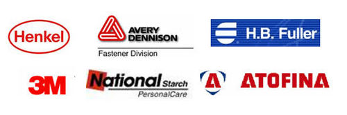
- Market leaders by company(which account for one-third of the market share) are:
- Henkel
- 3M
- Avery Denison
- HB Fuller
- National Starch
- Atofina
Intellectual Property
Patent Search Table
| ||||
| Query.No. | Searched Sections | Years Searched | Query | Hits |
| 1 | Claims, Title or Abstract | 1836 – Date | (rubber OR acryl* OR silicone OR oil*1 OR resin*1 OR ethylen* OR isoprene OR terpene OR copolymer* OR vinyl* OR siloxane* ((acid OR anhydride) ADJ1 (acrylic OR crotonic OR (vinyl ADJ1 acetic) OR fumaric OR maleic OR malonic OR succinic OR itaconic OR citraconic)) OR polymer* OR styrene OR ester*) SAME (((pressure ADJ1 sensitive) NEAR2 (adhesive* OR glue OR paste OR (binding ADJ1 agent) OR (epoxy ADJ1 resin*) OR film) OR PSA OR PSAs) OR (adhesion* WITH (peel OR tensile OR shear) OR stick*) OR (radical* ADJ1 (initiator* OR maker*))) | 76006 |
| 2 | Claims, Title or Abstract | 1836 – Date | (((low ADJ surface ADJ energy) WITH (substrate*1 OR polymer OR compound* OR material OR film)) OR (surface ADJ1 tension) OR (surface ADJ1 rough*) OR viscosity OR (oily ADJ surface) OR (low ADJ1 energy ADJ1 surface*)) AND (polyolefin*1 OR polyethylene*1 OR polypropylene*1 OR (polyvinyl ADJ1 chloride ADJ1 film) OR (oil ADJ1 contaminated ADJ1 metal) OR polybutene OR polyisoprene*1 OR (polyvinylidene ADJ1 fluoride*) OR polytetrafluoroethylene*1 OR polyester*1 OR polyamide*1 OR polyacetal*1 OR polystyrene*1 OR polyurethane* OR polyurea OR silan* OR polycarbonate*) | 75602 |
| 3 | Claims, Title or Abstract | 1836 – Date | 1 AND 2 | 2272 |
- Total number of patents - 2272
- Total number of unique patent families - 1483
Taxonomy for analysis

Taxonomy for PSA composition

IP Activity

Major Competitors

Composition components matrix
| Assignees | Rubber | Silicone | Polymers | Acrylic | Tackifying resin | Plasticizer oil | Carboxylic acids | Acid Esters | Priority Year | Patent numbers |
| 3M Innovative Properties Company | x | x | x | x | x | 2000 | US6630531 | |||
| x | x | x | x | 2000 | US6632872 | |||||
| x | x | 2000 | US6455634 | |||||||
| American Tape Company | x | x | 1997 | US5798175 | ||||||
| Ashland Oil, Inc. | x | x | x | 1991 | US5434213 | |||||
| Atlantic Richfield Company | x | x | x | x | 1984 | US4656213 | ||||
| x | x | x | x | 1996 | US5817426 | |||||
| x | x | x | 1996 | US5817426 | ||||||
| x | x | 1997 | US6461707 | |||||||
| Coloplast | x | x | x | 1980 | US6437038 | |||||
| Dow Corning Corporation | x | x | x | 1970 | US5916981 | |||||
| x | x | 1990 | US6337086 | |||||||
| x | 1990 | US6121368 | ||||||||
| x | x | 1994 | US5561203 | |||||||
| x | x | 1996 | US5861472 | |||||||
| Exxon Chemical Patents Inc. | x | x | 1993 | US5714254 | ||||||
| Fujikura Ltd. | 2000 | US6388556 | ||||||||
| General Electric Company | x | x | 2000 | US6387487 | ||||||
| H Fuller Licensing & Financing, Inc. | x | x | x | x | x | 1996 | US5741840 | |||
| H. B. Fuller Licensing & Financing, Inc. | x | x | x | 1997 | US5869562 | |||||
| Johnson & Johnson Products Inc. | x | x | x | x | 1981 | US4335026 | ||||
| Minnesota Mining and Manufacturing Company | x | x | x | 1993 | US5602221 | |||||
| x | x | x | 1993 | US5612136 | ||||||
| Nichiban Company Limited | x | 1997 | US6274235 | |||||||
| None | x | x | x | x | 1996 | US20030136510 | ||||
| PPG Industries, Inc. | x | x | x | x | 1996 | US5776548 | ||||
| Ralf Korpman Associates, Inc. | x | 1992 | US5760135 |
Technology Tree
As it is evident from the the technology tree below, although the IP activity in the area of Pressure sensitive adhesive was initiated during 1970s, companies are continuously trying new combinations of different components.

Key findings
- In the medical field, pressure-sensitive adhesive tapes are used for many different applications in the hospital and health areas and also they can be used to adhere two surfaces together such as the flaps of packing material or fabric to a surface
- In many commercial applications of pressure-sensitive adhesives, it would be preferred to use an acrylate polymer or copolymer having an intrinsic viscosity of at least about 2.5 dl/g
- Ideally, a process for producing an acrylate-based polymer for a pressure-sensitive adhesive provides a means for controlling both molecular weight, i.e., intrinsic viscosity, and molecular weight distribution.
- Pressure-sensitive adhesives require a delicate balance of viscous and elastic properties that result in a four-fold balance of adhesion, cohesion, stretchiness and elasticity. Pressure-sensitive adhesives generally comprise elastomers that are either inherently tacky, or elastomers or thermoplastic elastomers that are tackified with the addition of tackifying resins.